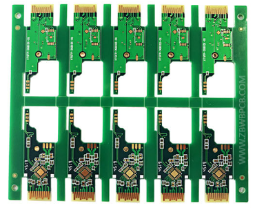
What is PCB? PCB is the abbreviation of printed circuit board (PCB board). Some countries call PCB PWB (printed wiring board).
PCB consists of an insulating substrate, copper foil for connecting wires, and pads for electronic soldering components.
It has the dual functions of conductive lines and insulating substrates, and can replace complex wiring to achieve circuit connections between components in the circuit.
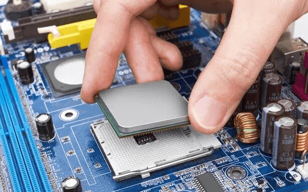
It is the motherboard of electronic components. Before the emergence of PCB, the interconnection between electronic components was done directly with wires,
But now wires only exist in laboratories for testing. It has occupied an absolute controlling position in the electronics industry.
After electronic equipment adopts PCB, due to the consistency of similar PCBs, manual wiring errors can be avoided, and electronic components can be automatically DIP or SMT,
Automatically soldered, and automatically detected, which ensures the quality of electronic equipment and improves labor productivity. In addition, it also reduces costs and facilitates maintenance.

What is PCB made of? The earliest used was paper-based copper-clad printed circuit boards. Since the emergence of semiconductor transistors in the 1950s, their demand has risen sharply. In particular, the rapid development and widespread application of integrated circuits have made electronic equipment increasingly miniaturized, and the density and difficulty of circuit wiring have continued to increase, which requires PWBs to be constantly updated. At present, the variety of PCBs has developed from single-sided to double-sided, multi-layer, and flexible PCBs, and the structure and quality of PCBs have also developed towards ultra-high density, miniaturization, and high reliability; new design methods, design supplies, PCB materials, and PCB manufacturing processes are constantly emerging. Various computer-aided design (CAD) PWB application software has been popularized and promoted in the PCB industry. In professional PCB manufacturers, mechanized and automated production has highly replaced manual work.
PCB production process
1. Cutting, rounding, planing and cutting are the process of cutting the original PWB copper-clad board into a work board that can be made on the production line.
Generally, it is cut into a work board of about 40*50cm.
2. VIA drilling, it is necessary to use a CNC drill to drill through the VIA holes on the top and bottom layers of the PWB.
3. PCB through-hole copper deposition, after drilling, the entire wall of the PCB material is free of copper, and a thin layer of copper needs to be deposited
On the surface of the PCB using the copper deposition process.
4. For PWB electroplating, there is a thin copper layer on the surface of the copper-immersed PCB, which does not meet the IPC bottom layer 18um copper thickness requirement,
So electroplating is required to increase the consistency of drilling. The production standard of the zbpcb factory is 20-26um.
5. PCB pressing, after pressing, a layer of dry blue film is pressed on the PWB. Dry film is a carrier, which is very important in circuit technology, so the dry film process is named after it.
Compared with wet film, dry film has higher stability and better quality, and can be used directly as non-metallized vias.
6. Circuit exposure: first align the circuit film of the pressed dry film with the PWB, and then place it on the exposure machine for exposure.
Under the energy of the exposure machine lamp, the dry film is exposed to the place where there is no circuit film. After the PWB circuit exposure process,
The place with the circuit is not exposed, and the place without the circuit is exposed.
7. Circuit etching: keep the copper that needs to be etched, and use sulfuric acid to etch away the copper where the copper does not need to be etched.
8. Make a PCB solder mask by screen printing or applying solder mask ink. Apply a layer of solder mask on the board to prevent short circuits during welding.
Usually use green, blue, red, white, and black solder masks.
9. PCB silk screen printing: print the position number of the component and the silk screen of the PWB model on the PWB, usually white or black silk screen printing.
10. PCB surface treatment, copper often exists in the form of oxides, which are easily oxidized by moisture when exposed to air for a long time,
And it is unlikely to keep the original copper color for a long time, so the copper surface needs to be treated.
The most basic purpose of surface treatment is to ensure good solderability or electrical performance.
11. PWB molding, the assembled board PNL is punched into the SET or PCS required to be shipped by CNC or mold, and the corresponding shapes V-cut, chamfer, step groove, tapered hole, etc.
Are processed.
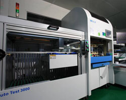
12. PCB testing, using PWB flying probe test or general test of electromechanical performance, check whether there are open or short-circuited NG boards.
Sometimes PCB impedance test and PWB high voltage test are also required.
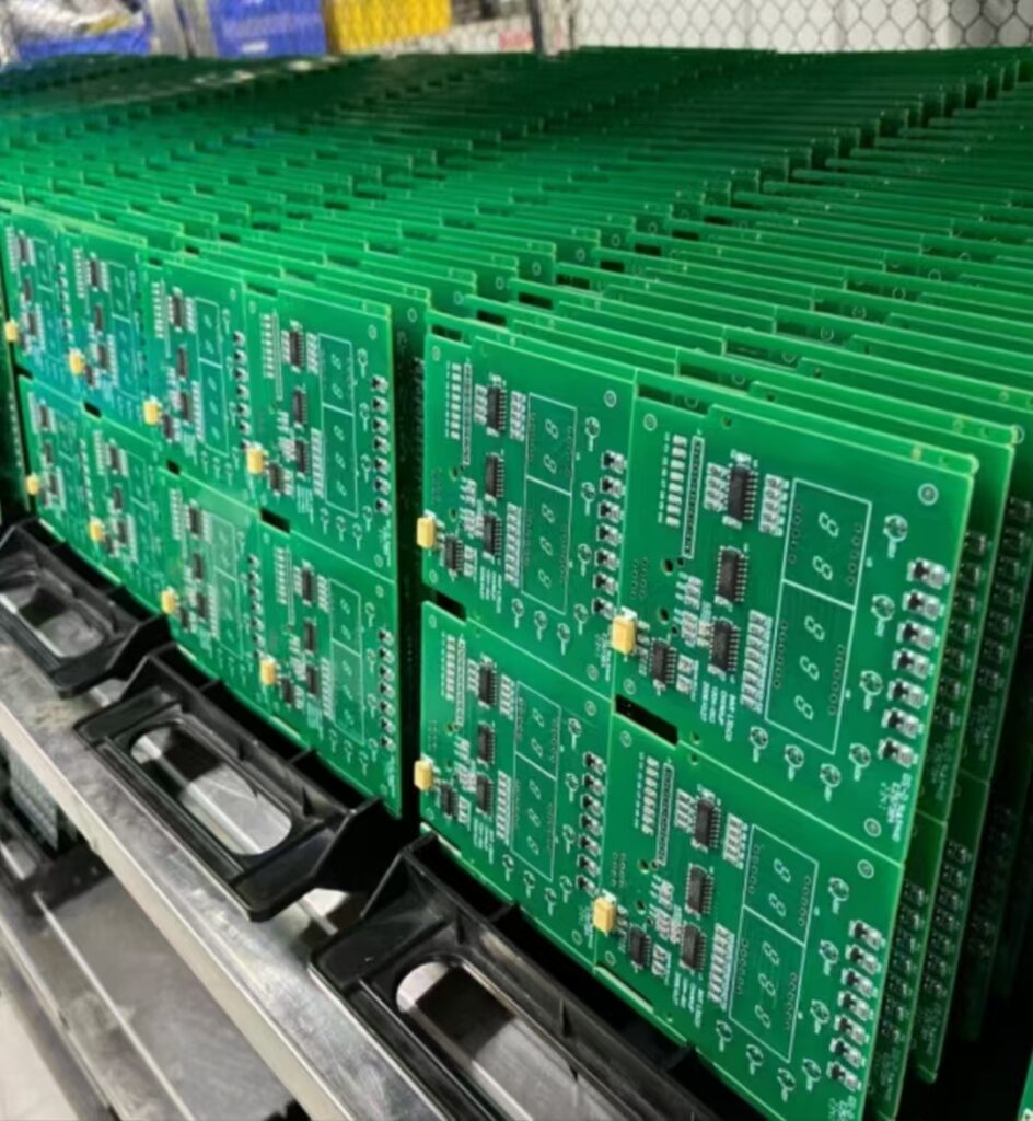
13. FQC final inspection, check whether the appearance, size, aperture, thickness, marking, etc. of the PCB meet customer requirements. Then, the qualified PWB is vacuum packed and shipped.
![]()
The role and characteristics of printed circuit boards.
1. Assembling. Printed circuit boards provide support for the fixing and assembly of electronic components, wiring, and electrical connection or insulation between electronic components on printed circuit boards, and provide the required electrical characteristics. Therefore, printed circuit board products can easily realize the standardized assembly of a variety of components, and can realize the automation and large-scale mass production of electronic products.
2. High reliability, providing a basis for the automation of DIP and SMT.
3. Productivity. When electronic equipment uses printed circuit boards, the consistency of printed circuit boards can avoid errors in manual wiring.
It can also realize the automatic insertion, automatic welding and automatic detection of electronic components, ensure the quality of electronic products, improve labor productivity, reduce costs, and facilitate maintenance.
4. Provide the required electrical, characteristic impedance and electromagnetic compatibility for circuit boards in high-speed or high-frequency circuits.
5. High production efficiency, circuit boards embedded with passive components provide certain electrical functions, simplify electronic installation procedures, and improve product reliability.
6. High density, providing an effective chip carrier for miniaturized chip packaging of electronic components in large-scale and ultra-large-scale electronic packaging components.
Common PWB design software providers include Altium, Cadence, Mentor, etc. Altium’s predecessor is Protel, and the successively launched Protel99SE, ProtelDXP,
And AltiumDesigner (AD) are widely used. Other commonly used software include pads, power PCB, MentorEE, allegro, CADENCE, Autocad, OrCAD, and Zuken CadStart.
Software used for PCB manufacturing includes Polar’s Genesis2000, CAM350, C-CAM/V2000, Cits25/si6000/si8000, etc. ZBPCB uses PCB design software to transfer Gerber files and uses
PWB manufacturing software for CAM processing.PWB is widely used, including consumer electronics, automotive electronics, semiconductor packaging, network communications, medicine, aerospace and other fields.
From the perspective of PCB demand, driven by the substantial growth in demand for new energy vehicles, automotive electronics, and PWB,
The demand for consumer electronics and semiconductor packaging is also very large.
PCB price calculation and PCB quotation
The price is composed of many factors
1. Different materials cause different pricesTake ordinary double-sided boards as an example. The board materials are generally FR4, CEM3, etc. The PWB thickness ranges from 0.6mm to 3.0mm, and the copper thickness ranges from ½Oz to 3Oz.
These have caused huge price differences on the board; in terms of solder mask ink,
There are also obvious price differences between ordinary thermosetting oil and photosensitive green oil, so the difference in materials causes the diversity of prices.
2. Different production processes cause different prices
Different production processes will cause additional costs, such as the production of gold-plated PCB boards and tin-sprayed PCB boards, milling PCB boards and beer (punching) PCB boards,
And the use of silk-screen circuits and dry film circuits will cause different PCB costs, resulting in different prices.
3. The difficulty of PCB manufacturing is different, and the price of PWB is also different
Even if the PWB material and process are the same, the difficulty of PWB itself is different, which will also cause different costs.
For example, if there are 1,000 holes on two circuit boards, and the hole diameter of one board is greater than 0.6mm, and the hole diameter of the other board is less than 0.6mm,
The drilling cost will be different; for example, if the two circuit boards are the same, but the line width and line spacing are different, one is greater than 0.2mm, and the other is less than 0.2mm,
The production cost will also be different, because the scrap rate of complex boards is higher, which will inevitably increase the cost and lead to price diversification.
4. Different customer requirements will also cause different prices
The level of customer requirements will directly affect the productivity of the board factory. For example, according to IPC-A-600E, IPC class2 requires a pass rate of 98%,
But the pass rate required by IPC class3 may be only 90%, which will cause different costs of blank circuit board factories, and ultimately lead to product price fluctuations.
5. Different PCB prices from different manufacturers
Different PCB manufacturers have different process equipment and technical levels. Even for the same product, other PWB costs will be different.
Many PCB manufacturers now like to produce gold-plated PCBs because the gold-plating process is simple and the cost is low,
But there are also manufacturers whose gold-plated PCB scrap rate will increase, resulting in higher prices, so they prefer to produce tin-sprayed PWBs,
So their quotes for tin-sprayed blank circuit boards are lower than gold-plated PWBs.
6. PCB price differences caused by different customer payment methods
At present, manufacturers generally adjust prices according to other payment methods, ranging from 5% to 10%, which also causes price differences. You can visit the circuit board factory ZBPCB.
7. PCB manufacturers are located in different regions, resulting in different prices
In terms of China’s geographical location, prices gradually increase from south to north, and there are specific differences in prices in different regions, so other regions also cause different PCB quotes.
How to calculate the PCB quotation?
1. Blank circuit board cost, different P costs, different PCB board costs are calculated separately. Circuit board costs are calculated separately.
1.1. Circuit board material: FR-4, CEM-3, this is our standard double-sided PWB and multi-layer PWB board,
its price is also related to the thickness of the board and the thickness of the copper platinum in the middle of the board, and FR-I, CEM-1 are our common PCB materials,
the price of this material is also very different from the double-sided PCB and multi-layer circuit board above.
1.2. It is the thickness of the PCB board. Its commonly used thicknesses are: 0.4, 0.6, 0.8, 1.0, 1.2, 1.5, 1.6, 2.0, 2.4, 3.0, 3.4. Our conventional board thickness and price are not much different.
1.3. The thickness of copper platinum will affect the price. The thickness of copper platinum is generally divided into 18um, 2/1OZ, 35um, 1OZ, 70um, 2OZ, 105um, 3OZ, 140um, 4OZ, etc.
1.4. PCB raw material suppliers, standard and commonly used ones are Shengyi, KB, Isola, TUC, etc.
2. PCB process cost. The process requirements of PCB boards are different, resulting in different PCB process difficulties, and even PCB prices will be different.
2.1. Depends on the circuit on the PCB, such as the wire density is less than 4/4mm, the price will be calculated separately.
2.2. There is also BGA on the board, so the cost will increase relatively, and BGA is another one in some places.
2.3. Depends on what the PCB surface treatment process is. Our common ones are lead tin spraying, hot air leveling, OSP, environmentally friendly board, pure tin spraying,
Tin plating, silver plating, and gold plating. Of course, the surface process is different. The price will also be different.
2.4. It also depends on the process standards. We usually use IPC2, but some customers have higher requirements and need IPC3. Of course, the higher the level, the higher the price.
3. Labor, water and electricity plus management expenses. This cost depends on the cost control of each PCB factory.
4. PCB drilling cost, the number of holes and the size of the aperture affect the drilling cost.
In the future, PCB will have the characteristics of high wiring density, small size and light weight, which is conducive to the miniaturization of electronic equipment.
In the environment where emerging technologies such as 5G communication, cloud computing, big data, artificial intelligence, Industry 4.0,
And the Internet of Things are accelerating, the PCB industry, as a factor connecting the entire electronic information manufacturing industry chain, will enter a technology and new product cycle.
The market demand for mid-to-high-end PCB products such as multi-layer PCB, HDI PCB, flexible PCB, rigid-flexible board, high-frequency PCB, high-speed PCB,
And IC carrier board is growing, and the production equipment of PCB manufacturing companies also needs to be updated accordingly.
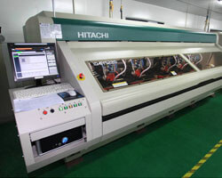
PCB manufacturers upgrade automated printed circuit board manufacturing equipment to obtain lower PCB manufacturing costs and better PCB board quality. Now, do you know? What is PCB?
PCB Directory for ZBPCB
 High-frequency printed circuit board | 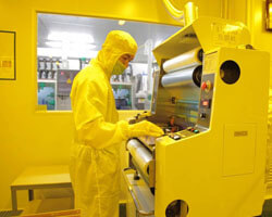 High-Speed printed circuit board | 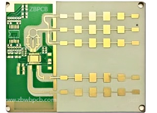 Multilayer printed circuit board |
 HDI PCB |
Rigid-Flex printed circuit board |
IC Substrate |
 PCB Assembly |
Standard printed circuit board | 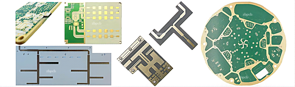 Special printed circuit board |