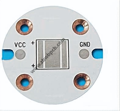
Counterbore hole pcb factory
Model : LED counterbore hole pcb
Material :aluminum base
Layer: 1Layers
Color : White/Black
Finished Thickness :1.2mm
Copper Thickness : 10z
Surface Treatment :Lead-free HASL
Thermal Conductivity:1.0w/m.k
Special process : counterbore hole pcb
Application : LED pcb
Countersunk hole is a blind hole machined from the surface of PcB to the interior of PcB. it is often used to install bolts or other connecting parts

PCB countersunk hole marking As electronic products develop towards light, thin, short and small, PCB must consider machine volume, shape,
Thickness and other issues in the process of assembling electronic components and designing the whole machine by the client,
Forcing PCB to develop towards higher precision wiring, lamination and special process design
In the design and manufacturing process of traditional printed circuit boards, in order to achieve and match the overall volume of the client,
Improve the product stacking structure and wiring density, and minimize the overall thickness of the circuit board,
But due to factors such as line width, spacing, and number of layers, the thickness reduction is limited in the design and manufacturing process
Generally, after the printed circuit board PcB! is delivered to the customer, electronic components will be assembled.
Electronic components are generally attached to the surface of the circuit board, so bulges will be generated, thereby increasing the volume of the whole machine.
Therefore, how to improve the structure of the circuit board and make it flatter has become a technical problem that needs to be solved in the field of PCB processing.
@ 2025 Zhibo Microwave Circuit Co., Ltd. All rights reserved